
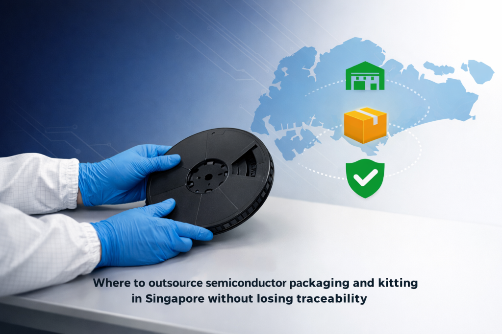
Semiconductor companies face mounting pressure to reduce costs, accelerate time-to-market, and manage supply chain complexity without building in-house packaging capabilities. Singapore has emerged as a strategic hub for contract manufacturing, offering ISO-certified facilities, regional logistics networks, and deep expertise in tape and reel packaging. This guide explains what contract manufacturing for semiconductor packaging involves, how to evaluate potential partners, and why integrated logistics capabilities matter for operational success.
Quick Summary
Contract manufacturing for semiconductor packaging involves outsourcing assembly, testing, and packaging operations to a specialized third-party provider. These services include tape and reel, carrier tape production, thermoformed trays, kitting, and logistics management. Companies use this approach when they need ESD-safe handling, EIA-481 standards compliance, or integrated warehousing and distribution support without building in-house capacity.
The global outsourced semiconductor assembly and testing (OSAT) market reached USD 44.1 billion in 2024 and is projected to grow at a CAGR of 8.9% through 2034. For semiconductor companies evaluating partners, understanding the scope of services, certifications, and logistics integration is essential to making an informed decision.
What Is Contract Manufacturing for Semiconductor Packaging?
Contract manufacturing for semiconductor packaging is the practice of outsourcing assembly, packaging, and logistics operations for semiconductor components to a specialized third-party provider, allowing companies to access expertise and infrastructure without capital investment.
This approach differs from wafer-level services provided by OSAT (Outsourced Semiconductor Assembly and Test) providers that handle die attach, wire bonding, and electrical testing. Contract packaging partners focus on component-level packaging for finished semiconductor devices, including tape and reel, thermoformed trays, carrier tape, kitting, and supply chain services.
The types of packaging handled by contract manufacturers include:
- Tape and reel packaging for surface mount devices
- Thermoformed trays and clamshells for component protection
- Carrier tape with ESD-safe properties
- Molded pulp for sustainable packaging applications
- Crates and pallets for shipping and warehousing
Contract manufacturers play a critical role in the semiconductor supply chain by bridging the gap between device fabrication and end-customer delivery. They provide the specialized equipment, cleanroom environments, and process expertise required for ESD-safe handling and standards compliance. For companies without dedicated packaging operations, this model offers a path to market without the capital expenditure of building in-house facilities.
SuperPak’s manufacturing services include thermoformed products, tape and reel packaging, and carrier tape production, all designed to meet the precision requirements of semiconductor applications.
Why Do Semiconductor Companies Outsource Packaging?
Semiconductor companies outsource packaging to reduce capital expenditure, access specialized equipment and expertise, accelerate time-to-market, and focus internal resources on core competencies like chip design.
The transition toward outsourcing allows manufacturers to concentrate on design and fabrication while leaving complex packaging processes to specialized providers. In 2024, over 55% of semiconductor devices produced globally featured advanced packaging techniques such as 3D IC and system-in-package solutions. These techniques require precision equipment and trained personnel that many companies find more efficient to outsource.
Beyond cost savings, outsourcing provides flexibility during demand fluctuations. Contract manufacturers can scale production up or down based on order volumes, eliminating the fixed costs associated with underutilized in-house capacity.
Cost and Capital Efficiency
Building in-house packaging facilities requires significant capital investment in cleanrooms, ESD-safe equipment, and trained personnel. Contract manufacturing converts these fixed costs into variable expenses that scale with production volume.
In-house semiconductor packaging facilities require specialized equipment for tape and reel production, thermoforming, and testing. These investments can reach millions of dollars before a single component is packaged. By outsourcing, companies redirect capital toward research, design, and market development while maintaining access to production infrastructure through their contract partner.
The total cost benefit extends beyond equipment. Contract manufacturers spread their overhead across multiple clients, achieving economies of scale that reduce per-unit costs for each customer.
Access to Specialized Expertise
Contract manufacturers bring decades of experience in handling moisture-sensitive components, ESD-safe packaging, and compliance with industry standards like EIA-481.
Semiconductor packaging requires adherence to multiple industry standards. EIA-481 defines the mechanical requirements for carrier tape, cover tape, and reels used in automated assembly. JEDEC standards govern moisture sensitivity classifications that determine floor life and dry-packing requirements.
Experienced contract manufacturers maintain current certifications, trained staff, and validated processes for handling these requirements. This expertise is difficult and expensive to develop internally, particularly for companies whose core competency is chip design rather than packaging operations.
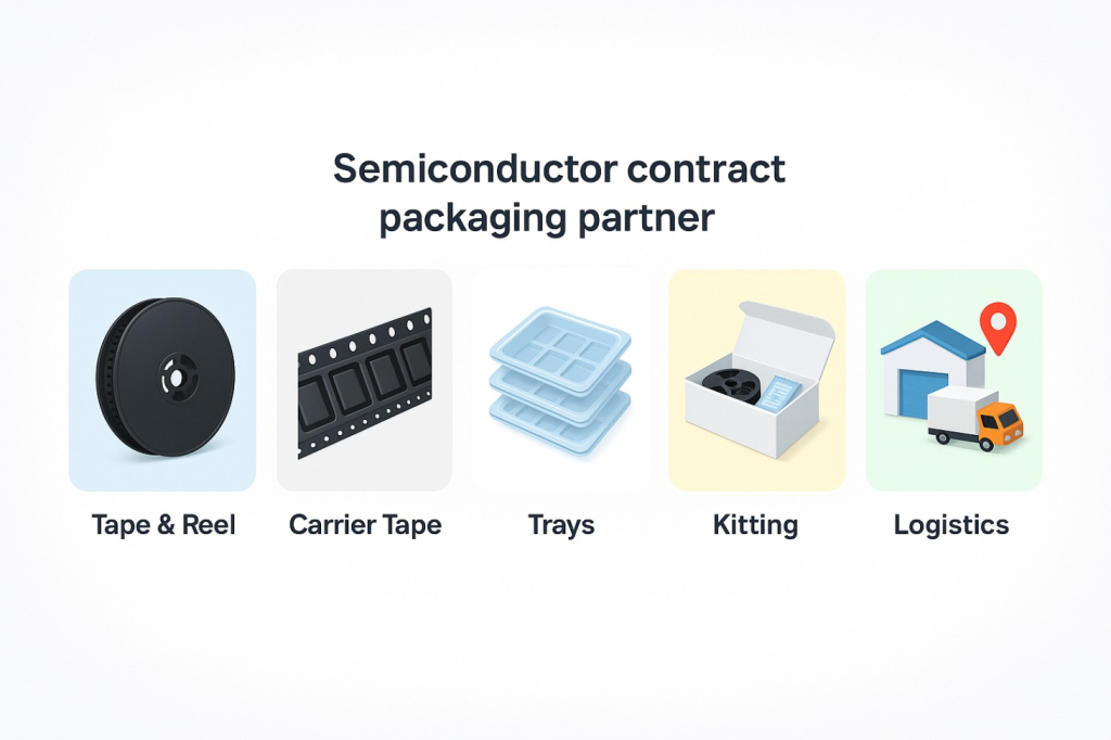
What Services Does a Semiconductor Contract Packaging Partner Provide?
A full-service semiconductor contract packaging partner provides tape and reel packaging, carrier tape manufacturing, thermoformed trays, kitting, assembly, testing, warehousing, and logistics management.
The scope of services varies by provider, but comprehensive partners offer end-to-end capabilities that span from product development through final delivery. This integration reduces handoffs between vendors, improves quality control, and simplifies supply chain management for OEM customers.
Tape and Reel Packaging
Tape and reel is the industry-standard method for packaging and transporting semiconductor components, where parts are loaded into carrier tape pockets, sealed with cover tape, and wound onto reels for automated pick-and-place assembly.
The process follows EIA-481 standards to ensure compatibility with surface mount assembly equipment. Carrier tape widths range from 8mm to 104mm, with pocket depths up to 19mm depending on component size. Cover tape must meet specified peel strength requirements, typically between 10 grams and 100 grams for 8mm tape.
Materials used for carrier tape include polystyrene (PS), conductive PS, APET, PP, and PC. The choice of material depends on component sensitivity and ESD protection requirements. SuperPak’s tape and reel products include carrier tape, cover tape, and plastic reels manufactured to meet these specifications.
Carrier Tape and Cover Tape Manufacturing
Carrier tape provides the precision pockets that hold semiconductor components during shipping and assembly, while cover tape seals the components in place until they reach the pick-and-place machine.
Carrier tape specifications vary by component type:
- Width: 8mm to 104mm
- Maximum formable depth: 19mm
- Materials: PS, conductive PS, APET, PP, PC, and permanent static dissipative clear PC
Cover tape is typically made from PET base film with antistatic or conductive surface treatment. Thickness ranges from 53 to 65 microns, and peel force is calibrated between 20g and 90g per millimeter. Cover tape must be heat-sealable or pressure-sealable depending on the application.
Kitting and Assembly Services
Kitting combines multiple components into ready-to-use sets, reducing assembly time at the OEM’s facility and simplifying inventory management.
For semiconductor applications, kitting may include combining carrier tapes with reels, documentation, and dry-packing materials into complete shipment packages. Assembly services extend to product configuration, testing, and labeling according to customer specifications.
SuperPak’s kitting services support medical, electronics, and industrial applications where precision and traceability are essential.
Warehousing and Logistics
Integrated warehousing and logistics services ensure just-in-time delivery, reduce lead times, and provide buffer stock management across regional supply chains.
Warehousing for semiconductor components requires controlled environments that maintain temperature, humidity, and ESD protection. Logistics services include inventory management, order fulfillment, and distribution to manufacturing sites across multiple locations.
SuperPak’s supply chain services provide warehousing, inventory planning, and distribution across Singapore, Malaysia, Indonesia, and China.
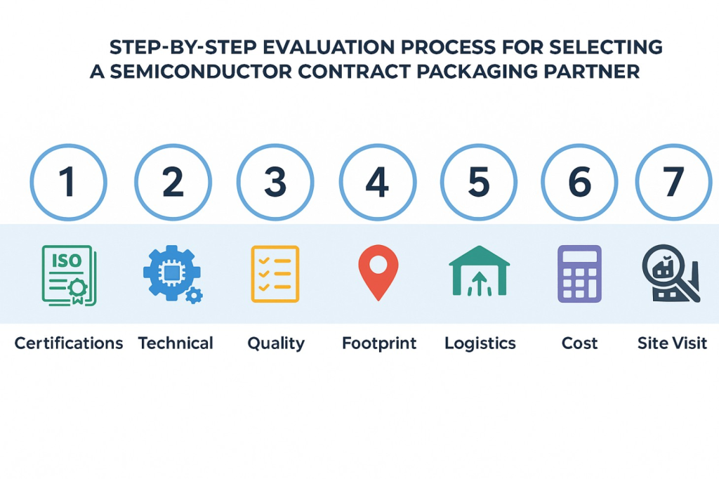
How to Evaluate a Semiconductor Contract Packaging Partner: Step-by-Step
Evaluating a semiconductor contract packaging partner requires assessing certifications, technical capabilities, quality management systems, regional footprint, and total cost of ownership across seven key criteria.
A structured evaluation process reduces risk and increases the likelihood of selecting a partner that meets both current requirements and future growth needs. The following framework addresses the critical factors that differentiate qualified partners from those that may introduce quality or supply chain problems.
Step 1: Verify ISO and Industry Certifications
Confirm that the partner holds ISO 9001:2015 for quality management and ISO 14001:2015 for environmental management. These certifications indicate systematic processes and third-party audits.
Additional certifications to verify include ESD-safe handling credentials and any industry-specific standards such as IATF 16949 for automotive or ISO 13485 for medical devices. Request copies of current certificates and verify they cover the specific facility and services you require.
Step 2: Assess Technical Capabilities
Evaluate the partner’s equipment for tape and reel production, thermoforming, and part-fit analysis. Confirm they can handle your specific component sizes, materials, and volume requirements.
Key technical specifications to verify:
- Carrier tape width range (8mm to 104mm for most applications)
- Maximum pocket depth capability
- Material options (PS, PC, APET, conductive materials)
- Testing equipment for peel strength and dimensional verification
Step 3: Review Quality Management Systems
Examine incoming inspection procedures, process controls, testing capabilities, and documentation practices. Request sample quality reports and traceability records.
Quality systems should include documented procedures for handling moisture-sensitive devices, ESD protection, and non-conformance management. Ask about yield rates, defect tracking, and continuous improvement programs.
Step 4: Evaluate Regional Manufacturing Footprint
Assess the partner’s locations relative to your supply chain requirements. Multiple regional facilities provide redundancy and reduce transportation costs.
Partners with facilities in Singapore, Malaysia, Indonesia, and China can serve the Asia Pacific market efficiently while providing options for business continuity planning. Proximity to your OEM facilities reduces lead times and simplifies logistics coordination.
Step 5: Examine Logistics and Supply Chain Integration
Evaluate warehousing capabilities, kitting services, and just-in-time delivery performance. Ask about inventory management systems and visibility tools.
Integrated logistics providers can hold safety stock, manage kanban replenishment, and coordinate shipments across multiple destinations. This integration reduces your internal logistics burden and improves responsiveness to demand changes.
Step 6: Calculate Total Cost of Ownership
Look beyond per-unit pricing to include tooling, shipping, duties, inventory carrying costs, and quality-related expenses in your evaluation.
Total cost of ownership components include:
- Tooling and setup costs
- Per-unit production costs
- Testing and inspection costs
- Packaging and shipping costs
- Import duties and taxes
- Inventory carrying costs
- Quality issue resolution costs
Step 7: Request References and Conduct Site Visits
Ask for references from customers in similar industries and schedule a facility visit to observe operations firsthand.
Site visits reveal operational details that cannot be captured in proposals or presentations. Observe cleanliness, equipment condition, worker training, and material handling practices. Ask to see quality records and speak with production staff about their processes.
Need a contract packaging partner that can meet today’s requirements and scale with your future demand? Contact SuperPak to align on your semiconductor packaging program and regional fulfillment needs.
Singapore vs. Other Regional Hubs for Semiconductor Contract Packaging
Singapore offers a unique combination of ISO-certified infrastructure, strategic location, skilled workforce, and government support that differentiates it from other regional semiconductor packaging hubs.
The table below compares Singapore with other major regional locations across key criteria:
Criteria | Singapore | Malaysia | Taiwan | China |
ISO Certification Prevalence | High (ISO 9001, 14001 common) | Moderate-High | High | Variable |
Logistics Infrastructure | World-class port, air connectivity | Good, lower cost | Excellent for wafer-level | Variable by region |
Labor Costs | Higher | Lower | Moderate | Lower |
IP Protection | Strong legal framework | Moderate | Strong | Concerns persist |
Government Incentives | Enterprise SG grants, R&D support | Investment incentives | OSAT subsidies | National semiconductor initiatives |
Proximity to OEM Facilities | Southeast Asia hub | Close to Singapore | East Asia hub | Domestic market focus |
English Proficiency | High | Moderate-High | Moderate | Lower |
Singapore’s semiconductor manufacturing sector generated over S$133 billion (approximately USD 101 billion) in 2023, contributing significantly to the country’s electronics output. The government has committed approximately S$18 billion (USD 13.6 billion) between 2021 and 2025 to support research, development, and innovation in the semiconductor sector.
Singapore’s strategic location provides access to Southeast Asian markets and efficient connectivity to China, Taiwan, Japan, and Korea. The Changi Airport and Port of Singapore offer reliable logistics options for time-sensitive shipments.
IP protection is particularly important for semiconductor companies sharing design information with packaging partners. Singapore’s legal framework and enforcement mechanisms provide stronger protection than many alternative locations.
Looking for an ISO-certified contract packaging partner with regional logistics capabilities? Contact SuperPak to discuss your semiconductor packaging requirements.
What Industry Standards Apply to Semiconductor Packaging?
Semiconductor packaging must comply with EIA-481 for tape and reel configurations, JEDEC standards for component handling, and ESD protection requirements under EIA-541 to ensure product integrity during assembly.
Understanding these standards is essential for both specifying requirements and evaluating partner capabilities. Non-compliance can result in assembly line failures, component damage, and customer rejections.
EIA-481: Tape and Reel Packaging
EIA-481 defines the mechanical requirements for carrier tape, cover tape, reels, and associated materials. The standard specifies dimensions, tolerances, and orientation rules for surface-mount components. Key requirements include:
- Sprocket hole pitch of 4.00mm
- Cover tape peel strength between 0.1N and 1.0N for 8mm tape
- Component orientation rules per EIA-783
- No missing components in consecutive positions
EIA-783: Component Orientation
EIA-783 specifies how components should be oriented within carrier tape pockets. Rules include placing the largest axis perpendicular to tape length and positioning pin 1 toward the sprocket holes.
EIA-541: ESD-Sensitive Packaging
EIA-541 defines packaging material standards for ESD-sensitive items. Carrier tape materials must provide appropriate static dissipation to protect semiconductor components during handling and storage.
JEDEC J-STD-020: Moisture Sensitivity
JEDEC J-STD-020 classifies moisture sensitivity levels (MSL) for non-hermetic surface-mount devices. Levels range from MSL 1 (not moisture sensitive) to MSL 6 (extremely moisture sensitive). Each level specifies floor life, the time components can be exposed to ambient conditions before requiring dry baking.
JEDEC J-STD-033: Handling and Storage
J-STD-033 defines procedures for handling, packing, and shipping moisture-sensitive devices. Requirements include dry-packing with desiccant and humidity indicator cards, along with proper labeling of moisture sensitivity levels.
Common Mistakes When Selecting a Semiconductor Packaging Partner
The most common mistakes in selecting a semiconductor packaging partner include focusing only on unit price, neglecting logistics integration, overlooking certifications, and failing to assess scalability for demand fluctuations.
Avoiding these pitfalls requires thorough due diligence and a comprehensive view of the partnership’s total impact on your operations.
- Prioritizing unit price over total cost of ownership – Logistics, duties, and inventory costs often exceed per-unit savings. A lower price from a distant supplier may cost more when shipping, lead times, and quality issues are factored in.
- Ignoring ISO and ESD certifications – Non-certified partners risk quality failures and customer rejections. Certifications provide evidence of systematic processes and third-party verification.
- Overlooking logistics capabilities – Warehousing and JIT delivery are essential for supply chain efficiency. Partners without these capabilities force you to manage inventory and distribution internally.
- Failing to verify standards compliance – EIA-481 and JEDEC compliance is non-negotiable for automated assembly. Non-compliant packaging causes line stoppages and rework costs.
- Not assessing scalability – Partners must handle volume fluctuations without quality degradation. Ask about capacity headroom and ability to ramp production quickly.
- Skipping site visits – Remote evaluations miss critical operational details. On-site observation reveals equipment condition, cleanliness, and worker competence.
- Neglecting sustainability requirements – OEMs increasingly require environmental certifications. Partners without ISO 14001 may be excluded from approved supplier lists.
- Underestimating communication barriers – Language and timezone alignment affect responsiveness. Ensure your partner can communicate effectively in your working language and hours.
What Does the Contract Manufacturing Process Look Like?
The contract manufacturing process for semiconductor packaging typically follows six stages: initial consultation, design and prototyping, pilot production, full-scale manufacturing, quality inspection, and logistics/delivery.
Understanding this process helps set expectations for timeline and milestones when engaging a new partner.
- Initial consultation and requirements gathering – Define component specifications, volume requirements, delivery schedules, and quality standards. Share technical drawings and sample components.
- Design and prototyping – The contract manufacturer develops carrier tape dimensions, selects materials, and creates prototype tooling. This stage includes design for manufacturability review.
- Part-fit analysis and simulation testing – Test components in prototype carrier tape to verify fit, orientation, and peel characteristics. Adjust dimensions as needed before production tooling.
- Pilot production run – Produce a limited quantity for validation. Test samples in actual pick-and-place equipment to confirm assembly compatibility.
- Full-scale manufacturing – Once pilot validation is complete, transition to full production. This stage includes process documentation, operator training, and production scheduling.
- Quality inspection and documentation – Inspect finished goods per agreed specifications. Generate quality records including lot traceability, inspection reports, and certificates of conformance.
- Packaging, warehousing, and delivery – Package finished reels with appropriate labeling and moisture protection. Store in controlled conditions and ship according to delivery schedule.
SuperPak’s product development services support the design and prototyping phases with part-fit analysis and simulation testing capabilities.
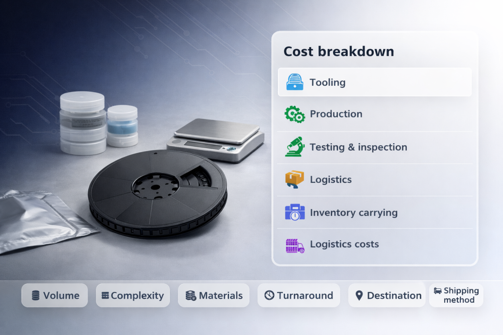
How Much Does Semiconductor Contract Packaging Cost?
Semiconductor contract packaging costs vary based on volume, complexity, materials, and logistics requirements. Total cost of ownership typically includes tooling, per-unit production, testing, and shipping.
Cost transparency is essential for accurate budgeting and supplier comparison. Understanding cost components helps identify opportunities for optimization.
Cost components to consider:
- Tooling costs – One-time charges for carrier tape molds and dies. Costs vary from several hundred to several thousand dollars depending on complexity.
- Per-unit production costs – Material and labor costs per reel or piece. Higher volumes typically yield lower per-unit costs.
- Testing and inspection costs – Quality verification including dimensional checks, peel testing, and visual inspection.
- Logistics costs – Shipping, insurance, customs clearance, and handling fees.
- Inventory carrying costs – Storage fees, insurance, and capital tied up in buffer stock.
Factors affecting pricing:
- Order volume and frequency
- Component size and complexity
- Material specifications (standard vs. specialty)
- Turnaround time requirements
- Destination and shipping method
When comparing quotes, ensure all cost components are included and specifications are equivalent. The lowest unit price may not represent the lowest total cost when logistics and quality factors are considered.
Sustainability in Semiconductor Contract Packaging
Sustainability in semiconductor packaging involves using recyclable materials, implementing closed-loop packaging programs, reducing waste, and achieving environmental certifications like ISO 14001.
OEMs increasingly require suppliers to demonstrate environmental responsibility. Contract packaging partners with established sustainability programs help their customers meet corporate environmental commitments.
Key sustainability initiatives include:
- Recyclable materials – Molded pulp, recyclable plastics, and biodegradable alternatives to conventional packaging materials.
- Closed-loop programs – Collection and refurbishment of reusable packaging items such as reels, trays, and shipping containers.
- Waste reduction – Process optimization to minimize material scrap and improve yield.
- ISO 14001 certification – Third-party verification of environmental management systems.
- Carbon footprint reduction – Energy efficiency improvements and renewable energy adoption.
SuperPak’s commitment to environmental sustainability includes ISO 14001:2015 certification and collection of packaging items for recycling and washing. The company’s blog covers biodegradable and recyclable packaging for semiconductor devices in the Singapore context.
Ready to request a quote for tape and reel packaging or contract manufacturing services? Get in touch with SuperPak’s packaging specialists.
Frequently Asked Questions
What is the difference between OSAT and contract packaging?
OSAT (Outsourced Semiconductor Assembly and Test) providers handle wafer-level packaging, die attach, wire bonding, and electrical testing. Contract packaging partners focus on component-level packaging such as tape and reel, carrier tape, kitting, and logistics for finished semiconductor devices. Some companies use both services at different stages of production.
What certifications should a semiconductor packaging partner have?
Essential certifications include ISO 9001:2015 for quality management, ISO 14001:2015 for environmental management, and ESD-safe handling credentials. Industry-specific certifications like IATF 16949 for automotive or ISO 13485 for medical devices may also be required depending on the application.
How long does it take to set up a contract packaging relationship?
Initial setup typically takes 4 to 12 weeks depending on complexity. This timeline includes consultation, design approval, tooling fabrication, pilot production, and quality validation. High-volume production can begin after pilot approval.
Can contract packaging partners handle small batch or prototype orders?
Many contract packagers offer high-mix/low-volume capabilities, making them suitable for prototyping, NPI (New Product Introduction), and small batch production. Confirm minimum order quantities and setup fees during the evaluation process.
What industries commonly use semiconductor contract packaging?
Primary industries include consumer electronics, telecommunications, automotive, medical devices, industrial automation, and aerospace. Each industry may have specific certification and compliance requirements.
How does integrated logistics reduce supply chain risk?
Integrated logistics combines warehousing, kitting, and just-in-time delivery under one partner, reducing handoff points, improving inventory visibility, and enabling faster response to demand changes. This consolidation minimizes transportation delays and communication errors.
What happens if a component is moisture-sensitive?
Moisture-sensitive components must be handled according to JEDEC J-STD-020 classifications, which specify floor life, dry-packing requirements, and bake-out procedures. Contract packagers should provide dry packing with humidity indicators and document moisture sensitivity levels on packaging labels.