
Not every electronic component fits neatly into a standard carrier tape pocket. When components are tall, irregularly shaped, or body-critical in ways that standard geometries cannot accommodate, off-the-shelf tapes introduce shifting, component damage, and pick-and-place failures that compound cost across the entire assembly line. This guide explains how custom deep pocket carrier tape is designed, specified, and validated, with a focus on what electronics manufacturers and semiconductor operations in Singapore need to know before committing to tooling.
Quick Summary
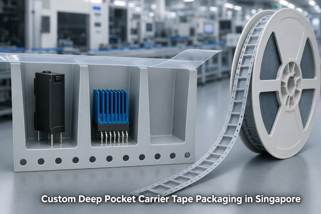
Custom deep pocket carrier tape is thermoformed carrier tape with pockets exceeding standard shallow-profile depths, designed to secure tall, bulky, or odd-form electronic components (such as connectors, relays, sensors, and heatsinks) during automated pick-and-place and transport. It is specified when a component’s height or body geometry cannot be reliably contained within a standard pocket. The key criteria are pocket depth, wall thickness uniformity, material ESD rating, and cover tape peel force compatibility. Caveat: custom tooling requires a validated part fit analysis before production approval.
What Is Deep Pocket Carrier Tape, and How Does It Differ from Standard Carrier Tape?
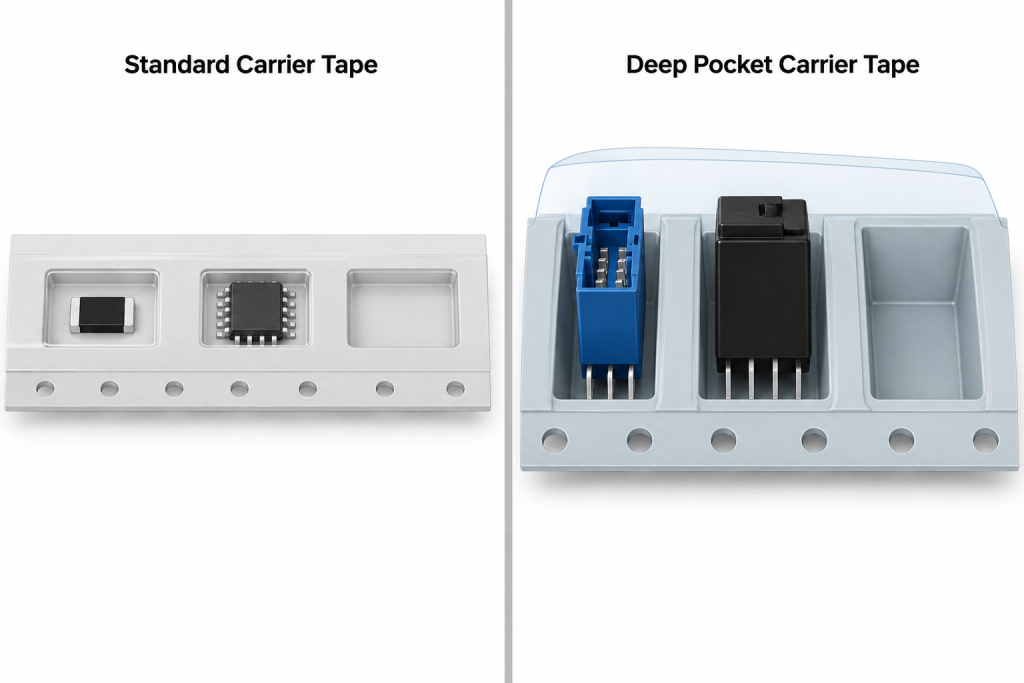
Deep pocket carrier tape is thermoformed carrier tape with pockets whose depth-to-width ratio significantly exceeds standard shallow-profile configurations, enabling reliable containment of taller or more complex electronic components. Standard carrier tape, governed by the ANSI/EIA-481-D standard for taping surface mount components, is optimised for flat or low-profile devices; deep pocket variants extend those depth limits to handle components that would otherwise tilt, shift, or be exposed at the pocket rim.
The fundamental engineering challenge is geometry. A standard 8 mm or 12 mm tape is designed for thin surface-mount passives and small ICs, where pocket depth requirements are modest. Once component height increases (whether from a tall discrete package, a connector body, or a heatsink-attached device) the same tape width and depth become inadequate. The component may protrude above the tape surface, making cover tape sealing unreliable, or it may rest at an angle inside the pocket, causing orientation errors at the pick-and-place head. Custom deep pocket design resolves all of these failure modes by engineering the pocket to match the specific component geometry from the start.
At Superpak, we manufacture carrier tape in-house across widths from 8 mm to 104 mm, with a maximum formable depth of 25 mm, using a range of materials including polystyrene (PS), conductive PS, APET, polypropylene (PP), polycarbonate (PC), and permanent static-dissipative clear PC.
The table below summarises the key differences between standard and deep pocket carrier tape:
Attribute | Standard Carrier Tape | Deep Pocket Carrier Tape |
Typical pocket depth | Shallow; suited for flat SMDs | Extended depth for tall or bulky component bodies |
Component types | Resistors, capacitors, flat ICs | Connectors, relays, sensors, heatsinks, tall discrete packages |
Tape widths supported | 8 mm to 56 mm (most common) | 16 mm to 104 mm and above |
Tooling requirement | Standard mould | Custom thermoforming tool per component geometry |
EIA-481 applicability | Fully standardised | Standard covers dimensions; custom depths require engineering sign-off |
Key failure risk if misspecified | Minimal for flat parts | Component tilt, shifting, cover tape lifting, pick-and-place errors |
Which Components Typically Require Deep Pocket Carrier Tape?
The primary trigger for specifying deep pocket carrier tape is component height, specifically, any component whose body height cannot be safely contained within a standard pocket without risk of tilt, cover tape contact, or physical interference during reel winding and transport.
The component families most commonly packaged in custom deep pocket carrier tape include through-hole-body connectors, power relays, industrial switches, tall sensor housings, heatsink-attached packages, optical modules, discrete power transistors, and certain BGA or LGA packages with elevated body profiles. Medical electronics sub-assemblies also frequently fall into this category, particularly where precision presentation and damage-free delivery to an automated assembly line are both mandatory.
Component lead geometry adds another dimension to the specification challenge. On leaded packages, poorly sized shallow pockets can compress or deflect leads during pocket loading or transport, introducing coplanarity defects that cause soldering failures downstream. The pocket must contain not just the body, but any protruding lead frame or termination features without contact damage.
For ESD-sensitive versions of these components, the requirement for custom deep pocket design intersects directly with material selection. Industry estimates suggest ESD may account for up to 33% of all semiconductor failures during manufacturing and handling, making the combination of correct pocket geometry and correct ESD-rated material a dual requirement — not two independent decisions.
If you are evaluating whether your component needs a custom deep pocket design, our part fit analysis and simulation testing service can determine the correct pocket specification from your component’s actual dimensions.
How Is Custom Deep Pocket Carrier Tape Designed?
Designing a custom deep pocket carrier tape is a structured engineering process: it begins with a 3D component measurement, moves through pocket geometry definition, material selection, tooling fabrication, and prototype thermoforming, and concludes with validated part fit testing before any production reel is approved. Skipping the validation stage is the single most common and most costly mistake in custom carrier tape procurement.
The nine-step process below reflects how we approach custom deep pocket design at Superpak, drawing on our in-house thermoforming and testing capabilities.
Step 1: Component measurement and data collection. Capture the full 3D dimensions of the component — length, width, height, lead or ball geometry, and any draft or protrusion features. A component drawing or physical sample is required at this stage; nominal datasheet dimensions are a starting point only, not a specification basis.
Step 2: Pocket geometry definition. Calculate pocket length (A0), width (B0), depth (K0), draft angles, bottom flat dimensions, and clearance tolerances using the component’s maximum body envelope — not nominal dimensions. Define sprocket hole pitch (P0), pocket pitch (P1), and the cover tape sealing zone relative to the pocket edge.
Step 3: Material selection. Choose the tape material based on ESD requirements, pocket depth, temperature exposure during storage and transport, and cover tape compatibility. Polycarbonate (PC) is generally preferred for deep pocket applications because of its higher rigidity and superior wall thickness distribution at depth compared to polystyrene.
Step 4: Tooling design and fabrication. Engineer and fabricate the custom thermoforming tool. Tool design accuracy (including tool material, temperature control capability, and draft geometry) directly determines pocket wall uniformity. Research published in the Journal of Thermal Engineering confirms that the most influential factors for pocket quality in thermoformed carrier tape are tool design, tool material, and heat transfer dynamics during forming.
Step 5: Prototype thermoforming and cross-section analysis. Run a small prototype batch and conduct cross-section cuts to verify wall thickness distribution. Thermoformed pocket walls are generally not uniform in thickness and often break during the forming process, making cross-section verification a non-negotiable quality gate for deep pocket designs.
Step 6: Part fit analysis. Load actual components into the prototype tape. Verify correct seating: no tilt, no excessive lateral play, no interference between the component body and the pocket walls. Simulate the pick-and-place nozzle engagement to confirm the component is presented at the correct height and orientation.
Step 7: Cover tape compatibility test. Verify peel force at the intended sealing temperature and confirm that the sealed cover tape clears the component’s highest point without contact. Peel force must fall within the range specified in ANSI/EIA-481-D to ensure reliable automated peeling without component loss.
Step 8: Ageing test (where required). Assess tape dimensional stability and peel force consistency after accelerated ageing. This step is required wherever components will be stored on reel for extended periods before assembly, or where temperature cycling during transit is expected.
Step 9: Production approval and reel winding. Once all validation tests are passed and documented, approve the design, run the production batch, wind tape onto the plastic reel, and pack in the reel box for shipment.
Ready to start a custom deep pocket tape design for your component? Contact Superpak to request a part fit analysis and quotation: our engineering team will work from your component drawing or physical sample.
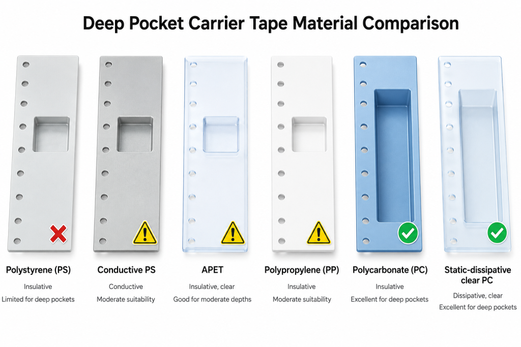
What Materials Are Used for Deep Pocket Carrier Tape?
The five core materials for custom deep pocket carrier tape are polystyrene (PS), conductive PS, APET, polypropylene (PP), and polycarbonate (PC), with permanent static-dissipative clear PC as a specialised variant for applications that combine ESD protection with visual inspection. Material choice is driven by ESD requirements, pocket depth, temperature tolerance, and cover tape sealing compatibility.
Material selection carries higher consequences in deep pocket applications than in standard shallow tape. As pocket depth increases, the thermoforming process stretches the polymer film further, and materials with lower rigidity or higher crystallinity (such as standard PS) become more susceptible to wall thinning, cracking, and dimensional drift at depth. This is not a theoretical concern: industry data shows thermoforming defects including uneven wall thickness can increase scrap rates to 5 to 15% in unoptimised processes, with deep-pocket geometries representing a disproportionate share of those defects.
The table below compares the six material options relevant to deep pocket carrier tape design:
Material | ESD Property | Typical Use Case | Deep Pocket Suitability | Cover Tape Compatibility |
Polystyrene (PS) | Insulative | Standard SMDs, non-ESD-sensitive parts | Limited (prone to wall cracking at high depth-to-width ratios) | Heat-activated adhesive |
Conductive PS | Conductive | ESD-sensitive components; standard depths | Moderate | Heat-activated adhesive |
APET | Insulative, clear | Visual inspection, moderate depths | Good for moderate depths | Heat-activated or PSA |
Polypropylene (PP) | Insulative | Flexible or medical-grade requirements | Moderate | Heat-activated adhesive |
Polycarbonate (PC) | Insulative | High-precision, tall-body components | Excellent (rigid, stable walls at depth) | Heat-activated adhesive |
Static-dissipative clear PC | Dissipative | ESD-critical components plus visual inspection | Excellent | Heat-activated adhesive |
Where both ESD protection and visual component inspection are required simultaneously, static-dissipative clear PC is typically the correct specification. The material’s optical clarity allows operators and automated vision systems to verify component presence and orientation inside the sealed tape without breaking the ESD protection barrier.
For a broader overview of how material selection interacts with tray and shielding bag choices across the semiconductor packaging system, see our guide on how to choose trays, tape and reels, and shielding bags for semiconductor companies in Singapore.
What Are the Key Dimensional Specifications for Deep Pocket Carrier Tape?
The critical dimensions for deep pocket carrier tape are pocket length (A0), pocket width (B0), pocket depth (K0), tape width (W), pocket pitch (P1), sprocket hole pitch (P0), and cover tape width — all defined relative to the component’s maximum body envelope plus defined clearance tolerances, not nominal dimensions. Specifying from nominal dimensions without clearance is the most frequent source of tooling rework.
Dimensional notation for carrier tape follows the ANSI/EIA-481-D standard. Each pocket dimension is calculated by adding a defined clearance value to the component’s maximum measured dimension in that axis. The sprocket hole geometry, pitch, and the cover tape sealing zone width must fit within the selected tape width without encroaching on the pocket boundaries. For deep pockets, the pocket depth (K0) also requires careful assessment of the draft angle: steeper draft angles ease component loading and release but reduce effective internal pocket volume, which may require compensating increases in pocket width or length.
Before submitting a custom tape specification to any supplier, confirm that your engineering team has addressed every item in the checklist below.
Pre-Specification Checklist:
- Component 3D drawing or physical sample is available, representing maximum body dimensions
- All critical dimensions confirmed: length, width, height, lead or ball geometry, any protrusion features
- Component ESD sensitivity class has been identified and documented
- Operating temperature range for storage and transport has been defined
- Pick-and-place nozzle size and engagement depth requirements have been confirmed
- Cover tape sealing method (heat-activated vs. pressure-sensitive adhesive) has been decided
- Reel size (7-inch or 13-inch) has been confirmed based on downstream equipment feeder specification
Completing this checklist before engaging a custom tape manufacturer prevents the most common delay, the need to revisit tooling after prototype part fit testing reveals a dimensional mismatch caused by an incomplete initial specification.
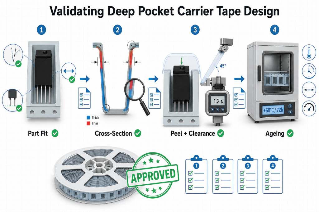
How Do You Validate That a Custom Deep Pocket Carrier Tape Design Is Correct?
Validating a custom deep pocket design requires three sequential, documented tests: a part fit analysis confirming correct component seating in the prototype tape, a cross-section analysis confirming wall thickness distribution, and a cover tape compatibility test confirming peel force consistency and component clearance. An ageing test is added when storage duration or temperature cycling is a concern.
These are not optional quality-assurance steps, they are the engineering basis for production approval. Moving to production without completing each test introduces risk that is disproportionately expensive to correct after tooling has been committed and production quantities have been ordered.
Each test serves a distinct purpose:
Part fit analysis confirms that the component seats correctly in the pocket: no tilt beyond the permitted angular deviation, no lateral movement exceeding the specified clearance, and no interference between the component’s body or leads and any pocket feature. The test uses actual physical components loaded into prototype tape, not dimensional calculations alone.
Cross-section analysis verifies the pocket wall geometry after thermoforming. For deep pockets, wall thickness is not uniform (material stretches more at corners and vertical walls than at the base) and cross-sections confirm whether wall thickness falls within the required minimum at every critical point. Research confirms that the temperature difference between the plastic film and the forming tool during thermoforming is the most significant variable affecting wall uniformity, making this test essential for any new deep pocket geometry.
Cover tape compatibility test measures peel force at the specified sealing temperature and confirms that the cover tape does not contact the component body when sealed over the deep pocket. The ANSI/EIA-481-D standard defines the peel force range within which a tape-and-reel system must operate for reliable automated handling.
Ageing test assesses whether tape dimensions and cover tape peel force remain within specification after accelerated ageing. This test is particularly important for components with long supply chain lead times, where reeled products may sit in warehouse storage for months before assembly.
All four of these tests are performed in-house at Superpak before any production approval is issued.
What Are the Most Common Mistakes When Specifying Custom Deep Pocket Carrier Tape?
The most common and costly mistakes in custom deep pocket carrier tape specification are using nominal component dimensions without clearance tolerances, underspecifying ESD requirements, choosing the wrong material for the pocket depth, and skipping prototype part fit validation before production. Each of these mistakes produces a distinct and expensive failure mode.
Understanding these pitfalls before initiating a custom tape project protects tooling investment and prevents delivery delays that ripple through component supply timelines.
Mistake 1: Specifying pocket dimensions from nominal component dimensions without tolerances. Nominal datasheet dimensions represent the target; actual component bodies vary within a manufacturing tolerance band. Pockets built to nominal dimensions will be correctly sized for some components and too tight for others, causing loading jams or component damage. Always specify from the maximum body dimensions plus a defined clearance per axis.
Mistake 2: Assuming a general “ESD-safe” label is sufficient for all components. ESD sensitivity classes vary across a wide range. Just 100 volts of ESD can destroy or degrade semiconductor devices designed to operate at voltages as low as 1.2 volts and many CMOS devices are sensitive to charges below 1,000 volts. Specifying the correct surface resistivity range (conductive, static-dissipative, or insulative) requires identifying the component’s ESD sensitivity class per ANSI/ESD S20.20 or IEC 61340-5-1, not relying on a supplier’s general material classification.
Mistake 3: Selecting polystyrene or APET for a high depth-to-width ratio pocket. These materials are suitable for standard and moderate depths, but at high depth-to-width ratios they are prone to wall thinning and corner cracking during thermoforming — two failure modes that only appear after tooling has been fabricated and prototypes have been run. Polycarbonate is the recommended material for deep pocket applications precisely because its mechanical rigidity resists these deformation failure modes.
Mistake 4: Proceeding directly to production without part fit validation. This is the single largest source of wasted tooling cost and component rework in custom carrier tape procurement. A part fit analysis identifies dimensional mismatches at the prototype stage, where corrections cost tool modification time, not entire production batches and re-shipment cycles.
Mistake 5: Not verifying cover tape interaction with the component body. In deep pockets, the sealed cover tape bridges a larger gap above the component surface than in standard tape. If the component’s highest point is not adequately below the tape sealing zone, the cover tape will bow into contact with the component during reel winding, potentially damaging leads, optical surfaces, or adhesive-sensitive areas.
Mistake 6: Confirming tape specifications without checking downstream equipment compatibility. Pocket pitch, sprocket hole dimensions, and reel hub diameter must match the pick-and-place feeder specification of the assembly equipment where the tape will be used. A tape that is dimensionally correct for the component but incompatible with the feeder causes the same production stoppage as a tape that is incorrectly sized.
How Does Cover Tape Work with Deep Pocket Carrier Tape?
Cover tape seals the loaded carrier tape to contain components during reel winding and transport, and must peel cleanly at a consistent, controlled force at the pick-and-place feeder. For deep pocket tapes specifically, cover tape selection and sealing parameters are more critical because the tape bridges a greater gap above the component, increasing the risk of either inadequate sealing or unintended component contact.
Two types of cover tape are used with carrier tape systems. Heat-activated adhesive (HAA) cover tape is sealed to the carrier tape surface by applying a defined combination of heat, pressure, and dwell time. It forms a durable bond well-suited to standard storage durations and temperature ranges. Pressure-sensitive adhesive (PSA) covers tape bonds under mechanical pressure alone, without heat, making it the appropriate choice for components sensitive to the elevated temperatures involved in heat sealing.
Peel force consistency is the single most important cover tape performance parameter for automated assembly. The ANSI/EIA-481-D standard defines acceptable peel force ranges, and any deviation outside that range, whether too low (causing components to escape the pocket during handling) or too high (causing pick-and-place feeder jams), results in assembly line stoppages.
The deep-pocket-specific risk is cover tape sagging. When a cover tape bridges a deep pocket, the distance between the tape’s sealing bond lines on either side of the pocket is greater than in a standard tape. Under reel winding tension, this can cause the tape film to deflect toward the component surface. If the component has protruding leads, an adhesive-coated upper surface, or optical elements, contact from the deflected cover tape causes damage that cannot be reversed at the assembly stage.
Cover tape compatibility testing, conducted before production approval, confirms both the peel force profile and the component clearance geometry. At Superpak, we perform this test in-house as a standard part of our custom carrier tape validation process. For components that also require ESD-rated cover tape, we stock static-dissipative cover tape options compatible with our conductive and dissipative carrier tape materials.
Unsure which cover tape is compatible with your component and custom pocket geometry? Contact Superpak — our team conducts in-house cover tape compatibility and peel force testing as part of the standard custom tape development process.
What Are the ESD Requirements for Deep Pocket Carrier Tape in Semiconductor Applications?
Deep pocket carrier tape for semiconductor applications must be manufactured from materials with verified surface resistivity within the range required by the component’s ESD sensitivity class and must be qualified in accordance with ANSI/ESD S20.20 or IEC 61340-5-1. A general “ESD-safe” label without a confirmed surface resistivity measurement against the applicable standard is not a sufficient qualification basis for semiconductor-grade applications.
The three ESD material classification tiers relevant to carrier tape are:
Insulative: Surface resistivity greater than 10¹¹ ohms per square. Insulative materials accumulate charge and do not provide any ESD protection. They are appropriate only for non-ESD-sensitive components.
Static-dissipative: Surface resistivity in the range of 10⁴ to 10¹¹ ohms per square. Dissipative materials allow charge to flow slowly and in a controlled manner, preventing rapid discharge events. This is the specification for most ESD-sensitive semiconductor components.
Conductive: Surface resistivity below 10⁴ ohms per square. Conductive materials allow rapid charge equalisation. They are specified for the most sensitive components where even the slow discharge characteristic of dissipative materials could cause damage.
Superpak manufactures carrier tape in conductive PS and permanent static-dissipative clear PC — the two ESD-rated material options most commonly specified for semiconductor-grade deep pocket applications. The static-dissipative clear PC variant additionally enables visual inspection of loaded components through the tape body without breaking the ESD barrier.
For semiconductor fabs and OSAT facilities operating to cleanroom standards, cleanroom compatibility must also be confirmed. This affects not only the tape material’s outgassing and particle generation profile, but also the cover tape adhesive and any coatings applied during manufacture. For a deeper treatment of how ESD packaging choices integrate across the full semiconductor packaging system, see our guide on choosing the right ESD-safe packaging for semiconductor applications.
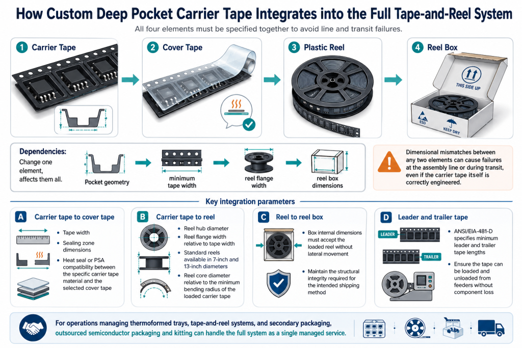
How Does Custom Deep Pocket Carrier Tape Integrate into the Full Tape-and-Reel System?
Custom deep pocket carrier tape is one component of a complete tape-and-reel system — and all elements of that system must be specified together. The full system comprises four elements: the carrier tape (with its custom deep pockets), the cover tape, the plastic reel, and the reel box. Dimensional mismatches between any two elements in this chain cause failures either at the assembly line or during transit, even when the carrier tape itself is correctly engineered.
Understanding how these four elements interact is essential before placing a custom order, because the carrier tape pocket geometry determines the minimum tape width, which in turn constrains the reel flange width, which constrains the reel box dimensions. Changing any one element after the rest have been specified often requires revision of the entire system.
The key integration parameters to confirm across the four system elements are:
- Carrier tape to cover tape: Tape width, sealing zone dimensions, and heat seal or PSA compatibility between the specific carrier tape material and the selected cover tape.
- Carrier tape to reel: Reel hub diameter, reel flange width relative to tape width (standard reels are available in 7-inch and 13-inch diameters), and the reel core diameter relative to the minimum bending radius of the loaded carrier tape.
- Reel to reel box: Box internal dimensions must accept the loaded reel without lateral movement, while maintaining the structural integrity required for the intended shipping method.
- Leader and trailer tape: ANSI/EIA-481-D specifies minimum leader and trailer tape lengths to ensure the tape can be loaded and unloaded from feeders without component loss.
For operations managing complex packaging across thermoformed trays, tape-and-reel systems, and secondary packaging, our outsourced semiconductor packaging and kitting service can handle the full system as a single managed service.
Why Source Custom Deep Pocket Carrier Tape from a Singapore-Based Manufacturer?
Sourcing custom deep pocket carrier tape from a Singapore-based manufacturer with in-house thermoforming, part fit analysis, and cover tape testing shortens design iteration cycles, eliminates cross-border logistics complexity, and supports the supply chain compliance requirements of OSAT facilities and electronics OEMs operating within the Singapore and broader ASEAN ecosystem.
Singapore’s position in the global semiconductor supply chain makes the local availability of precision packaging a supply chain advantage, not merely a logistical convenience. In 2025, Singapore’s semiconductor production expanded by 32.4%, driven by sustained demand for AI-related products and a significant concentration of back-end semiconductor operations in the city-state. Singapore captured approximately 20% of global semiconductor back-end services in 2025, supported by a cluster of OSAT facilities, advanced packaging operations, and electronics OEMs that all depend on precision component packaging supplied within short lead times.
For custom carrier tape specifically, the design-iterate-validate cycle is time-sensitive. Prototype thermoforming, part fit testing, and cover tape compatibility testing require multiple rounds of physical engineering before production approval. Conducting these rounds across a cross-border supplier relationship introduces shipping lead times, time zone delays, and communication gaps at every iteration point. A Singapore-based manufacturer with all validation capabilities in-house compresses each iteration from weeks to days.
Superpak has been headquartered in Singapore since 1985, with more than 40 years of precision packaging operations, dual ISO certification under ISO 9001:2015 and ISO 14001:2015, and a sustained focus on long-term supply partnerships with electronics and semiconductor clients. Our ISO 9001:2015 quality management certification documents the process controls governing every stage of custom carrier tape production, from tooling design through to final inspection and shipment. For a detailed explanation of what ISO 9001:2015 certification means for semiconductor packaging supply chain qualification, see our post on ISO 9001:2015 certified packaging providers for the semiconductor supply chain.
Our commitment to sustainability is equally concrete. Superpak’s ISO 14001:2015 environmental management certification reflects our focus on minimising carbon footprint through recyclable and biodegradable material options wherever technically compatible with packaging performance requirements. For electronics operations with sustainability reporting obligations, our packaging solutions support those commitments without compromising component protection.
Frequently Asked Questions
What is the maximum pocket depth available for custom carrier tape?
Pocket depth depends on tape width and material. Under ANSI/EIA-481-D, pocket depth limits vary by tape width, with wider tapes supporting substantially greater depths than narrow 8 mm or 12 mm tapes. Superpak’s in-house thermoforming capability supports a maximum formable depth of 25 mm. Polycarbonate is the recommended material for the deepest pocket geometries due to its superior wall rigidity during thermoforming. Contact us with your component height requirement and we will confirm whether it falls within our standard capability or requires a custom engineering assessment.
Can I receive a prototype tape sample before committing to a production order?
Yes, and for any custom deep pocket design, a prototype first-article run is a required engineering step, not an optional add-on. Superpak produces a prototype batch, conducts part fit analysis, cross-section testing, and cover tape compatibility testing before approving any production quantity. This protects your tooling investment and prevents the scenario of committing to a full production order before the design has been physically validated.
How do I determine what tape width my component needs?
Tape width is determined by the component’s largest footprint dimension, plus the pocket-to-tape-edge clearances defined in ANSI/EIA-481-D. Standard widths are 8, 12, 16, 24, 32, 44, and 56 mm; wider non-standard widths are available for large components. The correct width cannot be derived from body size alone — sprocket hole clearance zones, pocket pitch, and cover tape sealing width must all fit within the selected tape width. Our engineering team determines the correct tape width as part of the initial design proposal process.
What is the difference between heat-activated and pressure-sensitive cover tape?
Heat-activated adhesive (HAA) cover tape is sealed by applying heat and pressure at a defined temperature, forming a durable bond appropriate for most standard applications and storage conditions. Pressure-sensitive adhesive (PSA) cover tape bonds under mechanical pressure without heat, making it the correct specification for components that are sensitive to the elevated temperatures used in heat sealing. Both types must deliver consistent peel force within the range defined by ANSI/EIA-481-D for reliable automated pick-and-place performance.
What industries in Singapore use custom deep pocket carrier tape?
The primary users of custom deep pocket carrier tape in Singapore are semiconductor OSAT (outsourced assembly and test) facilities, electronics OEM contract manufacturers, industrial electronics producers, and medical device manufacturers handling precision electronic sub-assemblies. Singapore’s role as a regional semiconductor back-end hub — accounting for approximately 20% of global semiconductor back-end services in 2025 — drives strong local demand for precision carrier tape solutions tailored to complex and non-standard component geometries.
Can Superpak supply the complete tape-and-reel system, not just the carrier tape?
Yes. Superpak manufactures carrier tape, cover tape, and plastic reels in-house, and supplies all three as an integrated tape-and-reel system. This single-source approach ensures dimensional compatibility across the complete system (carrier tape width, cover tape sealing zone, reel flange width, and reel box dimensions) without the compatibility gaps that arise when components are sourced separately from different suppliers.