
Electrostatic discharge is one of the most persistent and expensive failure modes in semiconductor manufacturing. Industry estimates suggest ESD may account for up to 33% of all semiconductor failures during manufacturing and handling. For semiconductor companies in Singapore, where the sector generated over S$133 billion (US$101 billion) in 2023 alone, the financial risk of inadequate ESD packaging is substantial.
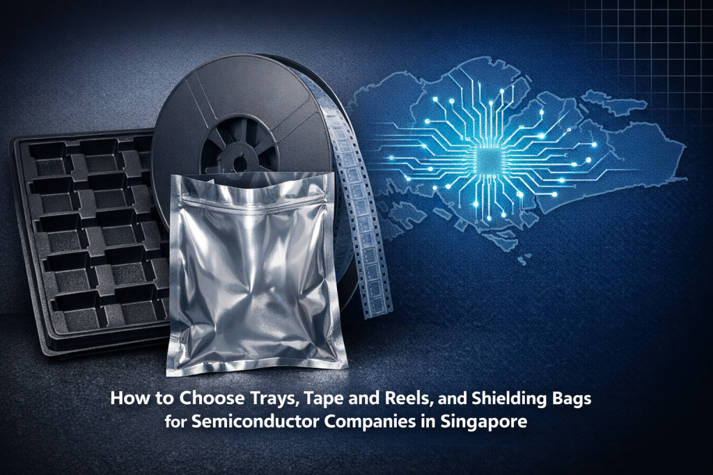
At SuperPak, we have been manufacturing custom packaging solutions from our Singapore headquarters since 1985, serving the semiconductor, electronics, and surface mount technology industries with thermoformed trays, carrier tape and reel systems, and engineered foam inserts. This guide covers everything semiconductor procurement and packaging engineers need to know about specifying, evaluating, and sourcing custom ESD safe packaging, from material science fundamentals to supplier selection criteria.
Quick Summary: What Is Custom ESD Safe Packaging for Semiconductors?
Custom ESD safe packaging for semiconductors is purpose-built protective packaging, including thermoformed trays, carrier tapes, foam inserts, and shielding bags, engineered from conductive or static-dissipative materials to prevent electrostatic discharge damage to sensitive components throughout manufacturing, transport, and storage.
This type of packaging matters because modern semiconductor devices can be destroyed by as little as 100 volts of ESD, while many operate at voltages as low as 1.2 volts. Off-the-shelf packaging often falls short for semiconductor-grade applications because it may not meet the required surface resistivity specifications, may not be cleanroom-compatible, or may lack the precision pocket geometries needed to protect delicate leads and die. Semiconductor fabs, outsourced assembly and test (OSAT) facilities, and electronics OEMs need packaging that is custom-fitted to their specific component dimensions and qualified to meet industry ESD protection standards such as ANSI/ESD S541 and IEC 61340-5-3.
Why Does ESD Protection Matter in Semiconductor Packaging?
Even a discharge as low as 100 volts can permanently damage modern semiconductor devices designed to operate at ultra-low voltages, making ESD safe packaging a non-negotiable requirement for any facility that manufactures, tests, stores, or ships ICs and wafers.
ESD damages semiconductors through two distinct failure modes. Catastrophic failure causes an immediate, permanent breakdown of the device’s circuitry, often visible under microscopic examination as burned or melted junctions. Latent defects are far more insidious: the discharge partially degrades the device without causing immediate failure, leading to premature field failures weeks or months later that are extremely difficult to trace back to ESD as the root cause.
The financial consequences are severe. The EOS/ESD Association estimates that 25% of all electronics damaged for unknown reasons can be attributed to ESD, and places the annual cost of ESD damage to the electronics industry at up to $5 billion (USD) per year. The cost of individual damaged devices ranges from a few cents for a simple diode to thousands of dollars for complex integrated circuits, and these figures increase sharply once rework, labour, logistics, and overhead are factored in.
The problem is getting worse, not better. As transistor geometries shrink below 10 nm and operating voltages continue to decrease, semiconductor devices become progressively more vulnerable to even minor electrical overstress. The EOS/ESD Association’s 2024 Technology Roadmap projects that charged device model (CDM) targets will drop from 250 volts to 125 volts by 2030, reflecting the increasing sensitivity of next-generation chips.
What Are the Key Types of ESD Safe Packaging for Semiconductors?
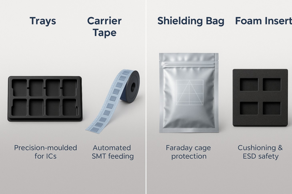
The four primary categories of ESD safe semiconductor packaging are thermoformed trays and clamshells, carrier tape and reel systems, ESD shielding bags and pouches, and conductive or dissipative foam inserts. Each serves a different stage of the semiconductor production and logistics chain, and many shipping solutions combine multiple types for layered protection.
Thermoformed Trays and Clamshells
Thermoformed trays are precision-moulded containers that hold semiconductor devices in individually pocketed cavities, protecting them during storage, in-process handling, and inter-facility transport. These trays are manufactured by heating a plastic sheet and forming it over a mould using vacuum or pressure, then CNC-machining or die-cutting to final dimensions.
At SuperPak, we produce thermoformed products using both vacuum forming and pressure forming techniques. Our forming capabilities accommodate a maximum area of W600mm x L1200mm x H400mm with formable thicknesses from 0.16mm to 10mm. Material options include conductive polystyrene (PS), APET, HIPS, PC, and permanent static-dissipative clear polycarbonate, all of which can be selected to meet specific ESD resistivity requirements for semiconductor handling.
Carrier Tape and Reel Systems
Carrier tape and reel is the standard packaging format for high-volume surface mount technology (SMT) components. Components are loaded into individual pockets in a carrier tape, sealed with a cover tape, and wound onto a reel for automated pick-and-place feeding on the SMT production line.
SuperPak manufactures carrier tape, cover tape, and plastic reels in-house. Our carrier tapes are available in widths from 8mm to 104mm with a maximum formable depth of 19mm, using materials including PS, conductive PS, APET, PP, PC, and permanent static dissipative clear PC. We also perform in-house part-fit analysis, cross-section analysis, and cover tape compatibility and ageing testing using precision equipment, so the packaging is fully qualified before production begins.
ESD Shielding Bags and Moisture Barrier Bags
ESD shielding bags create a Faraday cage effect that attenuates external electrostatic discharges and prevents them from reaching the component inside. This is a critical distinction from simple anti-static bags, which only reduce triboelectric charge generation on the bag’s surface but do not block external fields.
Moisture barrier bags (MBBs) add humidity protection for moisture-sensitive semiconductor devices, typically using multi-layer aluminised film constructions. For components classified under IPC/JEDEC J-STD-033, MBBs with desiccant packs and humidity indicator cards are essential to prevent moisture-related defects during reflow soldering. Many semiconductor shipping solutions use ESD shielding bags as outer packaging around components that are first placed in thermoformed trays or carrier tape reels.
Conductive Foam and Cushioning Inserts
Conductive and dissipative foam inserts, including expanded polyethylene (EPE) foam, provide both ESD protection and mechanical cushioning for fragile or irregularly shaped semiconductor components during transit. These inserts are typically die-cut or CNC-machined to the exact profile of the component, ensuring a snug fit that prevents movement while safely dissipating any accumulated charge.
ESD Packaging Material Comparison: Which Type Suits Your Application?
Selecting the right ESD packaging material depends on your component’s sensitivity class, the stage of handling (in-process versus shipping), cleanroom requirements, and whether you need intimate contact protection or Faraday-cage shielding from external fields.
The following comparison table summarises the key differences between the four primary ESD packaging types for semiconductor applications.
Criteria | Thermoformed Trays (Conductive PS / PC) | Carrier Tape and Reel | ESD Shielding Bags | Conductive Foam Inserts |
Primary use | Wafer/die/IC transport and storage | SMT pick-and-place feeding | Outer packaging for ICs and PCBAs | Cushioning inside boxes and crates |
ESD protection mechanism | Surface conductivity (dissipates charge) | Conductive or dissipative pocket walls | Faraday cage effect (blocks external fields) | Volume conductivity plus shock absorption |
Surface resistivity range | 10³ to 10⁵ Ω/sq (conductive) or 10⁶ to 10⁹ Ω/sq (dissipative) | 10³ to 10⁹ Ω/sq depending on material | Less than 10³ Ω/sq outer layer (shielding) | 10³ to 10⁵ Ω/sq |
Cleanroom compatible | Yes (low-particulate materials available) | Yes | Yes (low-outgassing variants) | Varies; specify low-lint grades |
Moisture barrier | No (add MBB for moisture-sensitive devices) | No | Yes (multi-layer MBB variants) | No |
Customisation level | High, moulded to component geometry | High, pocket dimensions per JEDEC or custom | Moderate, standard sizes with custom print | High, die-cut to component profile |
Reusability | High (washable, returnable) | Single-use (reel consumed by SMT line) | Limited (typically single-use) | Moderate |
Best for | High-value die, wafers, and modules | High-volume SMT components | Shipping and inter-facility transfers | Fragile or irregularly shaped components |
The resistivity classifications in this table follow the definitions in IEC 61340-5-3, where conductive materials have a surface resistance below 1 x 10⁴ Ω, static-dissipative materials range from 1 x 10⁴ to less than 1 x 10¹¹ Ω, and insulative materials exceed 1 x 10¹¹ Ω. In practice, many semiconductor shipping solutions combine multiple packaging types. For example, an IC may first sit in a conductive thermoformed tray, which is then sealed inside a shielding bag, and finally placed within a conductive foam-lined carton for transit.
What Standards Must ESD Semiconductor Packaging Meet?
ESD packaging for semiconductors must comply with IEC 61340-5-3 (packaging material classifications), ANSI/ESD S541 (packaging material requirements), and should be procured as part of a broader ESD control programme certified to IEC 61340-5-1 or ANSI/ESD S20.20.
The standards framework for ESD packaging operates on three levels. At the top, programme-level standards (ANSI/ESD S20.20 and its internationally harmonised equivalent IEC 61340-5-1) define the overall requirements for an ESD control programme, including training, compliance verification, grounding, and the use of appropriate packaging. These two standards are technically equivalent, with ANSI/ESD S20.20 being more prevalent in North America and IEC 61340-5-1 being the standard of choice across Europe, Asia, and the Middle East.
At the packaging-specific level, ANSI/ESD S541 (and its technically equivalent counterpart IEC 61340-5-3) defines the material properties, classifications, and test methods required for packaging used to protect ESD-sensitive items through all phases of production, transport, and storage . These standards classify packaging materials by their surface and volume resistance, shielding effectiveness, and charge generation properties.
For carrier tapes and trays used in automated semiconductor handling, relevant JEDEC standards define the dimensional and functional specifications that ensure compatibility with pick-and-place equipment. Singapore-based semiconductor facilities typically also require packaging to be compatible with their cleanroom environments per ISO 14644-1.
SuperPak holds both ISO 9001:2015 and ISO 14001:2015 certifications, which support supplier qualification processes for semiconductor customers who require documented quality management and environmental management systems from their packaging partners. For a deeper dive into how ISO certification applies to semiconductor supply chain procurement, see our guide on ISO 9001:2015 certified packaging providers for the semiconductor supply chain.
Standard | Scope | Regional Use |
ANSI/ESD S20.20 | Overall ESD control programme requirements | Primarily North America; globally recognised |
IEC 61340-5-1 | Overall ESD control programme requirements (harmonised with S20.20) | Worldwide, especially Europe and Asia |
ANSI/ESD S541 | Packaging material requirements for ESD-sensitive items | North America |
IEC 61340-5-3 | Packaging material classifications (technically equivalent to S541) | Worldwide |
JEDEC (various) | Carrier tape, tray, and reel dimensional standards | Worldwide |
ISO 14644-1 | Cleanroom classification | Worldwide |
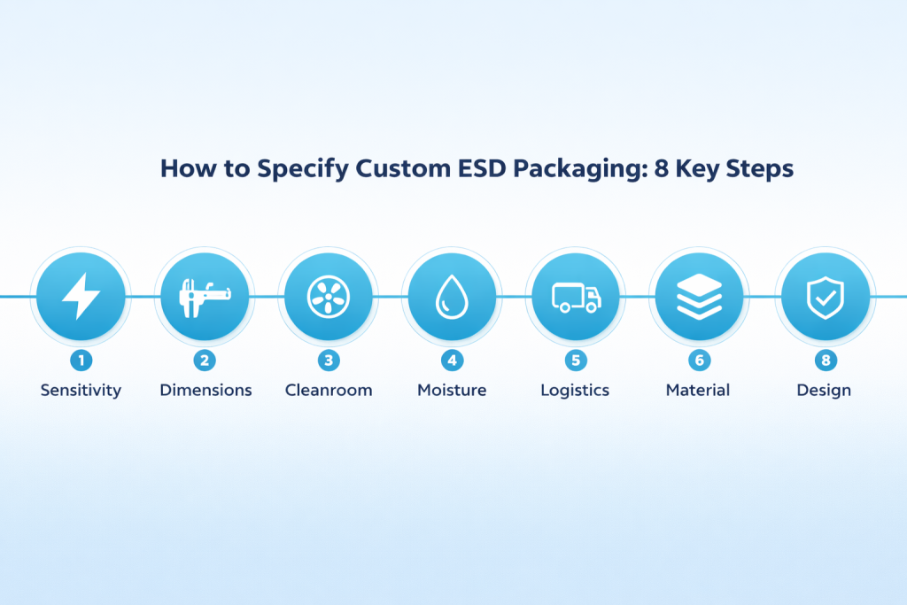
How to Specify Custom ESD Packaging: A Step-by-Step Process
Specifying custom ESD packaging requires defining the component’s ESD sensitivity class, physical dimensions, cleanroom grade, moisture sensitivity level, and logistics requirements before engaging a packaging manufacturer for design, prototyping, and qualification testing.
Follow these eight steps to move from initial requirements through to production-qualified packaging.
Step 1: Identify the component’s ESD sensitivity class. Check the device datasheet for human body model (HBM) and charged device model (CDM) withstand voltages. These values determine the minimum level of ESD protection your packaging must provide.
Step 2: Document physical dimensions and tolerances. Measure the component body, leads, bumps, and any keep-out zones. Record the weight per unit. For carrier tape applications, pocket dimensions must be tight enough to prevent component movement during reel advance, but loose enough to allow clean pick-and-place extraction.
Step 3: Determine cleanroom and contamination requirements. Specify the ISO cleanroom class for your packaging area, acceptable airborne particle counts, outgassing limits for packaging materials, and ionic contamination thresholds. Our guide to cleanroom packaging in Singapore covers these requirements in detail.
Step 4: Assess moisture sensitivity level (MSL). If the component is moisture-sensitive per IPC/JEDEC J-STD-033, specify whether moisture barrier bags, desiccant packs, and humidity indicator cards are required as part of the packaging solution.
Step 5: Define logistics and handling conditions. Document the shipping distance, vibration and drop requirements, temperature and humidity ranges during transit, and stacking or palletisation needs.
Step 6: Select material and packaging type. Use the comparison table from the previous section to match your requirements to the appropriate packaging category and material. For intimate packaging (material in direct contact with the device), dissipative materials are generally preferred over conductive materials to minimise CDM discharge risk.
Step 7: Engage a packaging manufacturer for design and prototyping. Provide the complete specification package and request part-fit analysis and simulation testing. At SuperPak, our Design Centre uses CAD/CAM tools to develop initial concepts, followed by CNC-machined prototype tooling for evaluation samples.
Step 8: Qualify the packaging. Conduct surface resistance testing per IEC 61340-5-3 test methods, perform drop and vibration testing to validate mechanical protection, and verify contamination levels meet your cleanroom specifications. Only after packaging passes qualification should it be approved for production use.
Ready to specify your custom ESD packaging? Contact SuperPak’s design team to start your project with a complimentary design consultation and quotation.
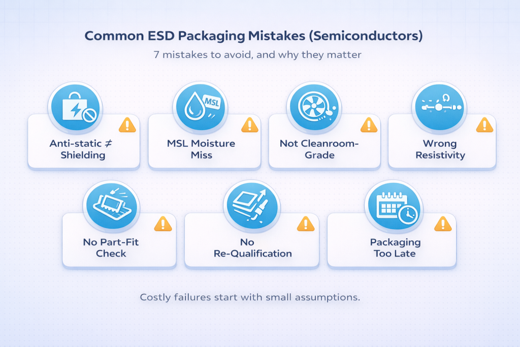
What Are the Most Common ESD Packaging Mistakes Semiconductor Companies Make?
The most costly ESD packaging mistakes in semiconductor operations include using anti-static material where shielding is required, neglecting humidity control for moisture-sensitive devices, failing to test packaging after material or design changes, and assuming that “pink poly” alone provides adequate protection for sensitive ICs.
Here are seven mistakes we see regularly, along with the consequences of each.
1. Confusing anti-static with static-shielding. Anti-static (or “pink poly”) bags reduce triboelectric charge generation on the bag surface, but they do not block external ESD events from reaching the component inside. For semiconductor ICs being transported outside an ESD Protected Area, shielding packaging that creates a Faraday cage is required per ANSI/ESD S541. Using anti-static bags where shielding is needed leaves components vulnerable to damage from external discharges during handling and shipping.
2. Ignoring moisture sensitivity level (MSL). Shipping moisture-sensitive components without appropriate moisture barrier bags, desiccant, and humidity indicator cards can lead to absorbed moisture causing “popcorning” during reflow soldering, resulting in cracked die or delaminated packages.
3. Using non-cleanroom-grade packaging in fab environments. Consumer-grade plastics can shed particles and outgas volatile compounds that contaminate sensitive semiconductor surfaces. Packaging materials used in or near cleanrooms must be selected and verified for low particulate generation and low outgassing.
4. Over-specifying or under-specifying resistivity. IEC 61340-5-3 notes that dissipative materials are preferred for intimate packaging in situations where CDM is a concern. Choosing highly conductive intimate packaging when dissipative would be more appropriate can actually increase CDM discharge risk to the device. Conversely, using insulative material within an ESD Protected Area defeats the purpose of the controlled environment.
5. Skipping part-fit validation. Poorly toleranced tray pockets or carrier tape cavities allow components to shift during handling, leading to mechanical damage such as bent leads, chipped substrates, or scratched die surfaces. Proper part-fit analysis before production approval is essential.
6. Not re-qualifying packaging when switching materials or suppliers. ESD properties can change significantly with formulation changes, different additive concentrations, or manufacturing process variations. Any material change requires retesting to IEC 61340-5-3 specifications.
7. Treating packaging as an afterthought. Specifying packaging late in the product development cycle severely limits optimisation opportunities. Engaging a packaging partner early in the design phase allows for concurrent engineering that optimises both protection and cost.
How Does Singapore’s Semiconductor Ecosystem Benefit from Local ESD Packaging Partners?
Singapore’s semiconductor ecosystem, home to major fabrication and OSAT facilities, benefits from local ESD packaging partners through shorter lead times, just-in-time delivery, reduced shipping risks, and the ability to iterate on custom designs without international logistics delays.
Singapore is a globally significant semiconductor hub. The country contributes more than 10% of total global semiconductor output and approximately 20% of worldwide semiconductor equipment production. In 2025, the Singapore semiconductor market reached an estimated USD 10.16 billion and is forecast to climb to USD 14.15 billion by 2030 at a 6.9% CAGR. The Singaporean government has committed approximately S$18 billion (US$13.6 billion) between 2021 and 2025 to foster research, development, and innovation within the sector.
This concentration of semiconductor activity creates strong demand for ESD packaging that can be prototyped, produced, and delivered rapidly. A local packaging manufacturer offers several concrete advantages for companies operating within this ecosystem. Prototyping cycles are shorter when design reviews can happen face-to-face and prototype samples do not need to clear customs. Just-in-time delivery across Singapore’s industrial zones (Jurong, Tampines, Woodlands, and others) reduces the need for large packaging buffer stocks. And when engineering changes are required, a local partner can turn around revised samples within days, not weeks.
SuperPak’s regional manufacturing footprint extends beyond Singapore to include facilities in Johor (Malaysia), Batam (Indonesia), and operations in China, providing supply chain resilience while keeping the centre of gravity close to Singapore’s semiconductor cluster. This regional presence also supports sustainability objectives: shorter transport distances reduce carbon emissions, which aligns with our ISO 14001:2015 environmental management certification and broader commitment to recyclable and biodegradable packaging materials.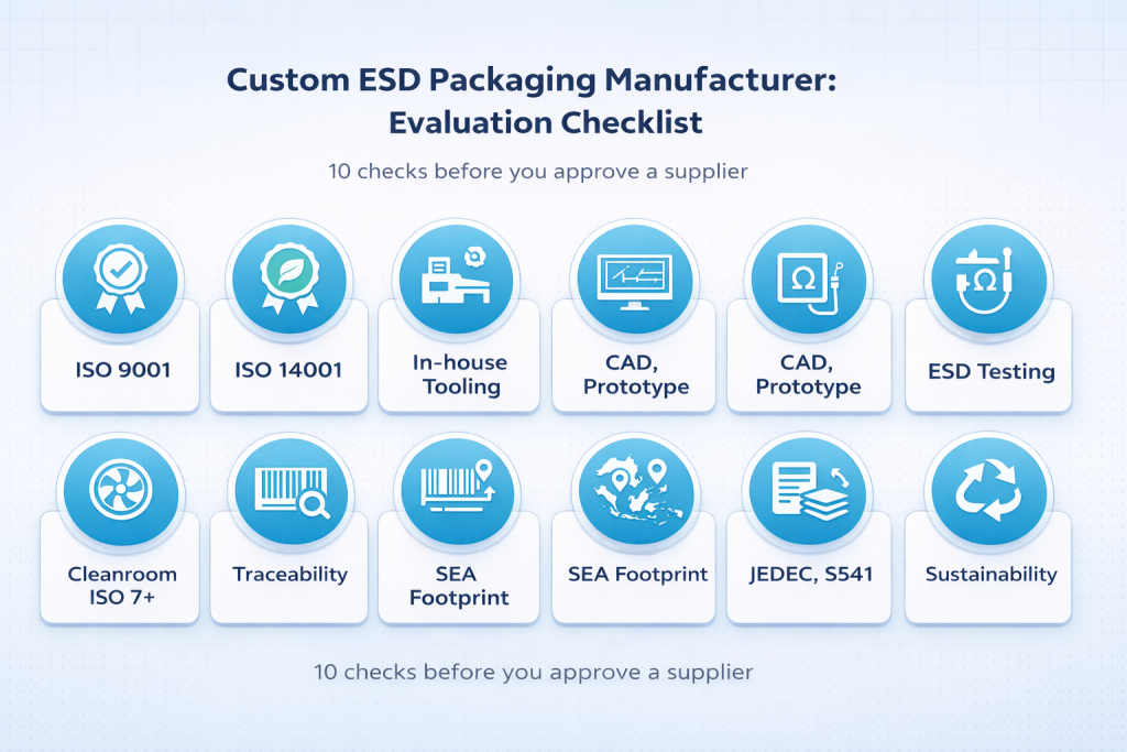
What to Look for in a Custom ESD Packaging Manufacturer: Evaluation Checklist
When evaluating a custom ESD packaging manufacturer for semiconductor applications, prioritise ISO certifications, in-house tooling and design capability, material traceability, cleanroom production zones, and the ability to conduct ESD resistance testing on finished packaging.
Use the following 10-point checklist when comparing potential suppliers.
- ISO 9001:2015 quality management certification to ensure documented, auditable quality processes across design, production, and delivery.
- ISO 14001:2015 environmental management certification to verify the supplier’s commitment to sustainable operations and waste reduction.
- In-house tooling and forming capability including thermoforming (vacuum and pressure forming) and carrier tape forming, so that design and production are controlled under one roof.
- Dedicated design centre with CAD/CAM and rapid prototyping for developing custom tray, tape, and insert designs without relying on third-party tooling shops.
- In-house or third-party ESD testing and part-fit analysis to verify that finished packaging meets IEC 61340-5-3 resistivity requirements and that components fit within specified tolerances.
- Cleanroom-grade production capability (ISO 7 or better) for packaging that will be used in or near semiconductor fabrication environments.
- Material traceability and lot-level documentation to support root cause analysis and provide audit trails required by semiconductor customers.
- Regional manufacturing footprint for supply chain resilience and the ability to serve multiple production sites across Southeast Asia.
- Proven experience with semiconductor industry standards including JEDEC tray and tape specifications and ANSI/ESD S541 / IEC 61340-5-3 compliance.
- Sustainability credentials including recyclable or biodegradable material options and returnable packaging programmes.
SuperPak meets every criterion on this checklist. We hold ISO 9001:2015 and ISO 14001:2015 certifications, operate an in-house design centre and testing lab, manufacture across Singapore, Malaysia, Indonesia, and China, and have served the semiconductor industry for over 40 years. For a detailed comparison of how to evaluate packaging providers against these criteria, read our guide on ISO 9001:2015 certified packaging providers for the semiconductor supply chain.
Looking for a packaging partner that ticks all the boxes? Share your requirements with SuperPak and receive a quotation tailored to your semiconductor packaging needs.
How Is Custom ESD Packaging Designed and Manufactured?
Custom ESD packaging is designed through an iterative process of component analysis, CAD modelling, CNC-machined prototype tooling, material selection and testing, pilot production, and full qualification, typically spanning four to eight weeks from initial brief to approved samples.
The process begins with our Design Centre, where engineers analyse the component’s physical characteristics and ESD requirements to develop a conceptual design. CAD models are created and reviewed with the customer before prototype tooling is CNC-machined from aluminium for rapid turnaround.
For thermoformed products, SuperPak uses both vacuum forming and pressure forming processes. Vacuum forming is ideal for simpler geometries and thinner gauges, while pressure forming achieves sharper detail and tighter tolerances for complex semiconductor components. Our thermoforming capabilities accommodate a maximum forming area of W600mm x L1200mm x H400mm, with formable material thicknesses from 0.16mm to 10mm. After forming, parts are die-cut or CNC-machined to final dimensions, and secondary processes such as barcode labelling or assembly can be performed as needed.
For carrier tape applications, we form pockets in widths from 8mm to 104mm with a maximum depth of 19mm. Cover tape is available in PET base with antistatic or conductive surface treatments, in thicknesses from 53 to 65 microns and peel forces from 20g to 90g/mm. Before production, we perform part-fit analysis, cross-section analysis, and cover tape compatibility testing in-house to verify that the complete tape-and-reel system functions correctly on the customer’s pick-and-place equipment.
Sustainability in ESD Packaging: Can You Be ESD-Safe and Eco-Friendly?
Yes. Modern ESD safe packaging can incorporate recyclable thermoplastics, biodegradable pulp-based materials, and returnable or washable tray systems that reduce waste without compromising electrostatic protection, provided the materials are tested to confirm they still meet IEC 61340-5-3 requirements.
Many of the core materials used in ESD packaging, including polystyrene (PS), PET, and polypropylene (PP), are widely recyclable. The sustainable ESD packaging segment alone was estimated at USD 1.66 billion globally in 2023 and is expected to grow at a 7.1% CAGR through 2030, reflecting increasing industry demand for eco-friendly alternatives.
Returnable tray programmes represent one of the most effective approaches to sustainable ESD packaging. Thermoformed trays can be washed, inspected, and reused across multiple shipping cycles, dramatically reducing per-unit packaging waste. SuperPak also offers moulded pulp packaging as a biodegradable alternative for applications where the material can meet the required ESD specifications, and provides collection and recycling services for used packaging items. For a comprehensive overview of sustainable options, see our guide on biodegradable and recyclable packaging for semiconductor devices in Singapore.
One important caveat: not all “green” materials are automatically ESD-safe. Any sustainable or recycled material must be independently tested and qualified to IEC 61340-5-3 specifications before it can be approved for semiconductor packaging use. Sustainability should complement, never replace, rigorous ESD qualification testing.
Frequently Asked Questions About ESD Safe Packaging for Semiconductors
What is the difference between anti-static and ESD shielding packaging?
Anti-static packaging reduces triboelectric charge generation on the material surface but does not block external electrostatic fields. ESD shielding packaging (such as metallised bags) creates a Faraday cage that attenuates external discharges, preventing them from reaching the component inside. For semiconductor ICs being shipped outside an ESD Protected Area, shielding packaging is required per ANSI/ESD S541.
What ESD packaging standards apply to semiconductor components?
The primary standards are IEC 61340-5-3 (packaging material classifications and requirements), ANSI/ESD S541 (packaging material requirements for ESD-sensitive items), and IEC 61340-5-1 / ANSI/ESD S20.20 (overall ESD control programme requirements). Carrier tape and tray dimensions may also need to comply with relevant JEDEC standards for automated handling compatibility.
How long does it take to develop custom ESD packaging for a new semiconductor product?
Timelines vary depending on complexity, but a typical custom thermoformed tray or carrier tape project, from initial specification through design, prototyping, qualification testing, and first production, takes approximately four to eight weeks. Factors that influence timelines include the number of design iterations, testing requirements, and tooling complexity. Contact SuperPak for a project-specific estimate.
Can ESD safe packaging also provide moisture protection for semiconductor devices?
Standard conductive or dissipative trays and carrier tapes do not provide moisture barrier protection on their own. For moisture-sensitive semiconductor devices classified under IPC/JEDEC J-STD-033, multi-layer moisture barrier bags with desiccant packs and humidity indicator cards should be used as outer packaging in combination with ESD-safe inner packaging.
What surface resistivity is required for ESD safe semiconductor packaging?
Per IEC 61340-5-3, conductive packaging materials have a surface resistance below 10⁴ Ω, and static-dissipative materials range from 10⁴ to less than 10¹¹ Ω. For intimate packaging in direct contact with semiconductor devices, dissipative materials are generally preferred to minimise charged device model (CDM) discharge risk.
Is it possible to get recyclable or sustainable ESD safe packaging?
Yes. Many ESD safe packaging materials, including PS, PET, and PP, are recyclable. Returnable tray programmes further reduce waste. However, any sustainable material must be tested and qualified to confirm it still meets IEC 61340-5-3 ESD requirements before use with semiconductor components.
Why should Singapore semiconductor companies use a local ESD packaging manufacturer?
Sourcing from a local manufacturer offers shorter prototyping and production lead times, reduced transit risks, easier face-to-face design collaboration, and just-in-time delivery capability. A Singapore-based partner with additional regional plants also provides supply chain resilience and lower carbon footprint from reduced shipping distances.
Next Steps: Getting Started with Custom ESD Packaging from SuperPak
Getting started with custom ESD packaging is straightforward. Share your component specifications, ESD sensitivity class, and volume requirements with our team, and we will provide a design concept and quotation, typically within days.
Here is how it works:
- Share your specifications. Email us your component dimensions, ESD sensitivity class, cleanroom requirements, volume forecasts, and any relevant standards or customer specifications at sales@superpak.com.sg.
- Receive a design concept and quotation. Our Design Centre will develop an initial packaging concept, recommend materials and formats, and provide a detailed quotation.
- Approve the prototype and begin production. After part-fit analysis and qualification testing confirm the design meets your requirements, we move directly into production from our Singapore or regional facilities.
With over 40 years of packaging manufacturing experience, ISO 9001:2015 and ISO 14001:2015 certifications, and a regional footprint spanning Singapore, Malaysia, Indonesia, and China, SuperPak is equipped to be your long-term ESD packaging partner.
Contact SuperPak today to discuss your custom ESD packaging requirements.